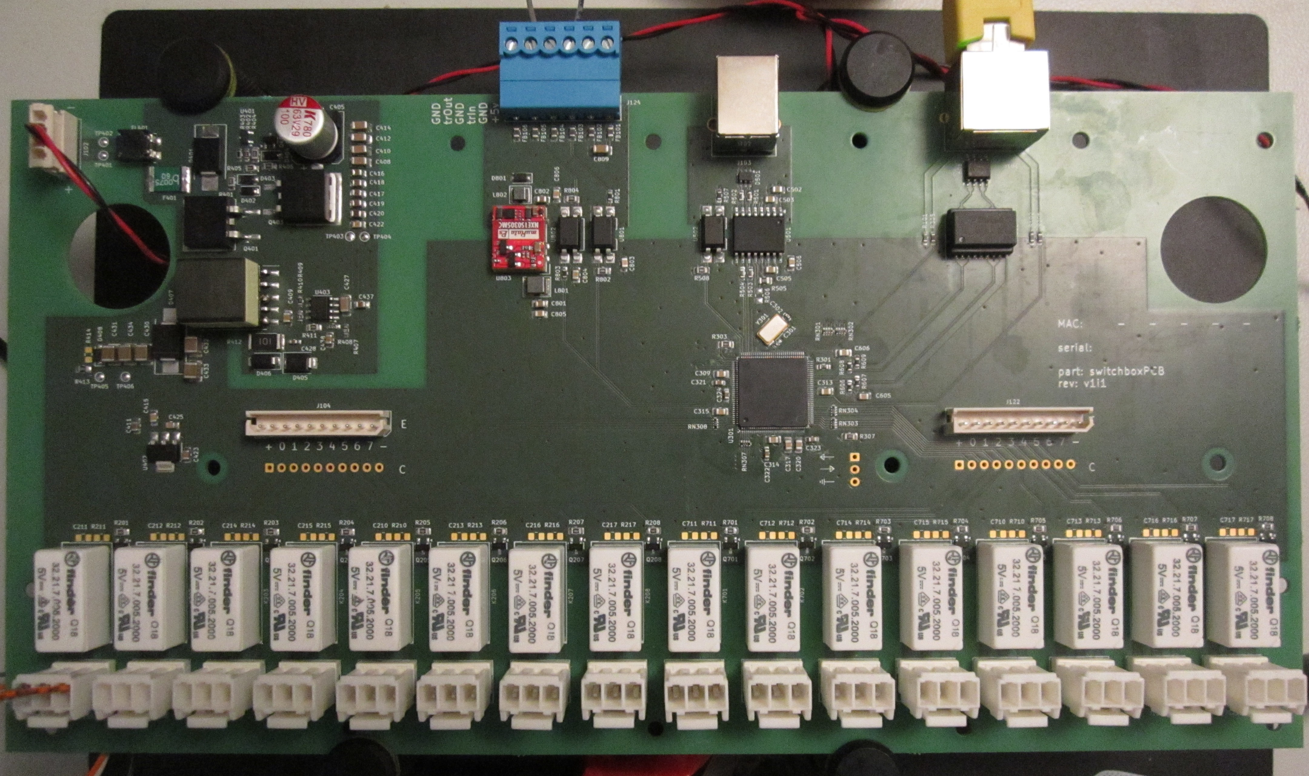
project: switchBox
hardware interfaces
power input
the device is powered by a 24VDC input. the input is fitted with a self resetting fuse, reverse polarity protection, a 36V overvoltage lockout, and a 18V undervoltage lockout.USB
the USB interface is galvanically isolated from every other interface.USB is a secondary control interface and ethernet should be preferred. USB may however be the most convenient way of configuring the ethernet interface connection parameters(i.e. DHCP or if not, the TCP/IP settings)
ethernet
the ethernet interface is the primary control interface and is a standard connectionswitches
the switches are electromechanical relays(finder 32.21.7.005.2000)| voltage rating | current rating | engage time(ms) | disengage time(ms) |
|---|---|---|---|
| 400VAC 250VDC | 6AAC 3A@24VDC .35A@110VDC .2A@220VDC | 2/10 NO/NC | 10/2 NC/NO |
trigger
a 5v logic trigger in and out are provided along with an exported 5v (150mA max) supplycontrol interfaces
both the ethernet and USB interfaces reach the same logical command processor interface. this is reached at port 5025 on ethernet and the CDC ACM on the USBcommand structure
the command structure roughly follows- *IDN?
- *RST
- *OPC?
- *SAV
- CONTact
- CLOSe[?] bank,contact
- OPEn[?] bank,contact
- TOGgle bank,contact
- COUNt? bank,contact
- SYSTem
- NETwork
- MAC?
- IP?
- NETwork
- TRIGger
- OUTput
- FORCe
- WIDth[?] [widthms]
- INVert[?] [(ON|OFF)]
- CHANENable[?] bank,contact
- CHANDISable[?] bank,contact
- PASSThrough[?] [(ON|OFF)]
- INput
- FORCe
- IGNore[?] bank,contact
- CLOSe[?] bank,contact
- OPEn[?] bank,contact
- TOGgle[?] bank,contact
- OUTput
history
the original 3d rendering before a masive rethink of the structure is below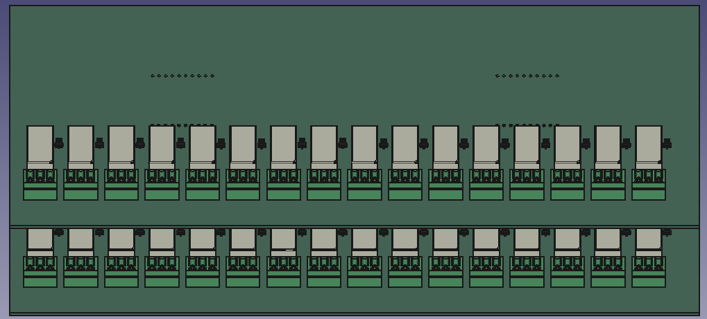
a rendering from before the PCB was reviewed and faults were found(this also predates the trigger system)
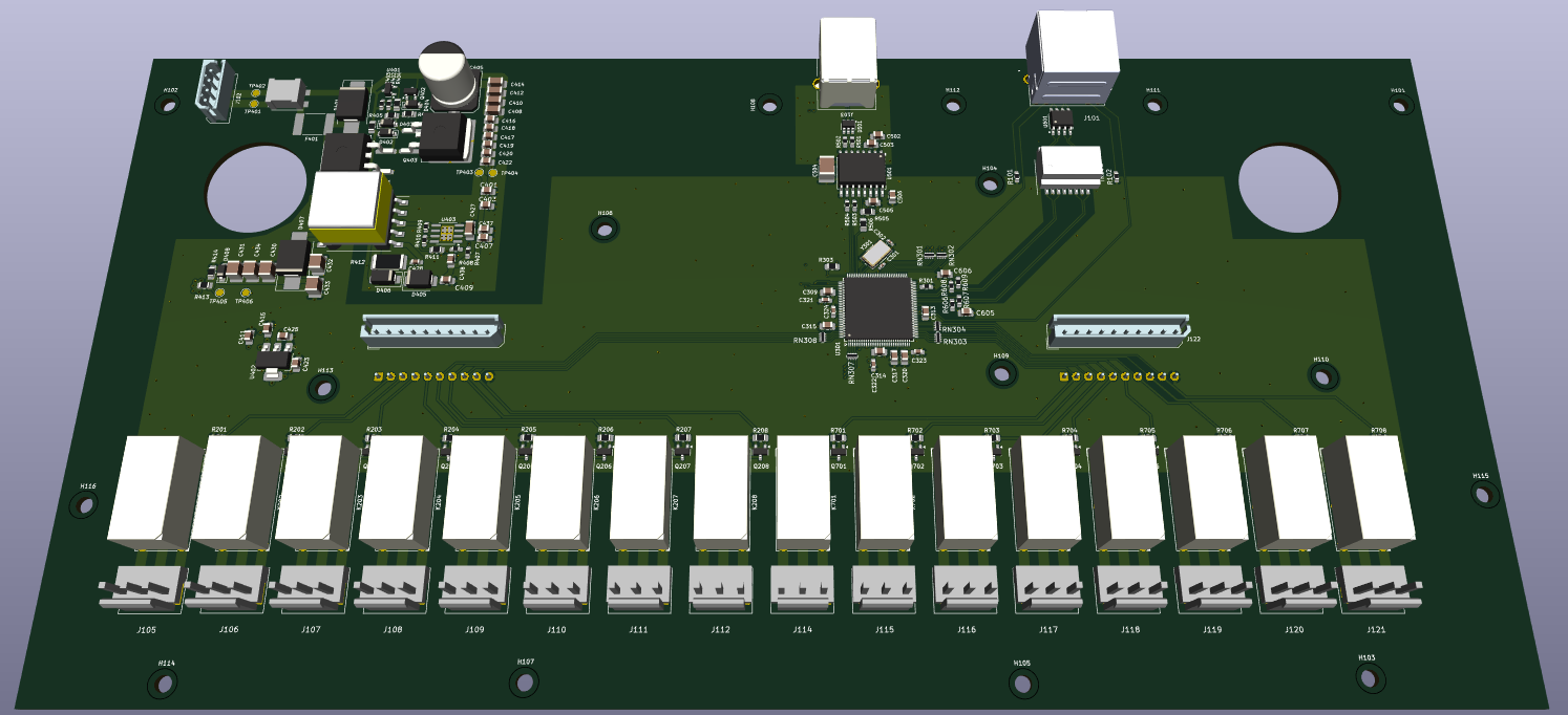
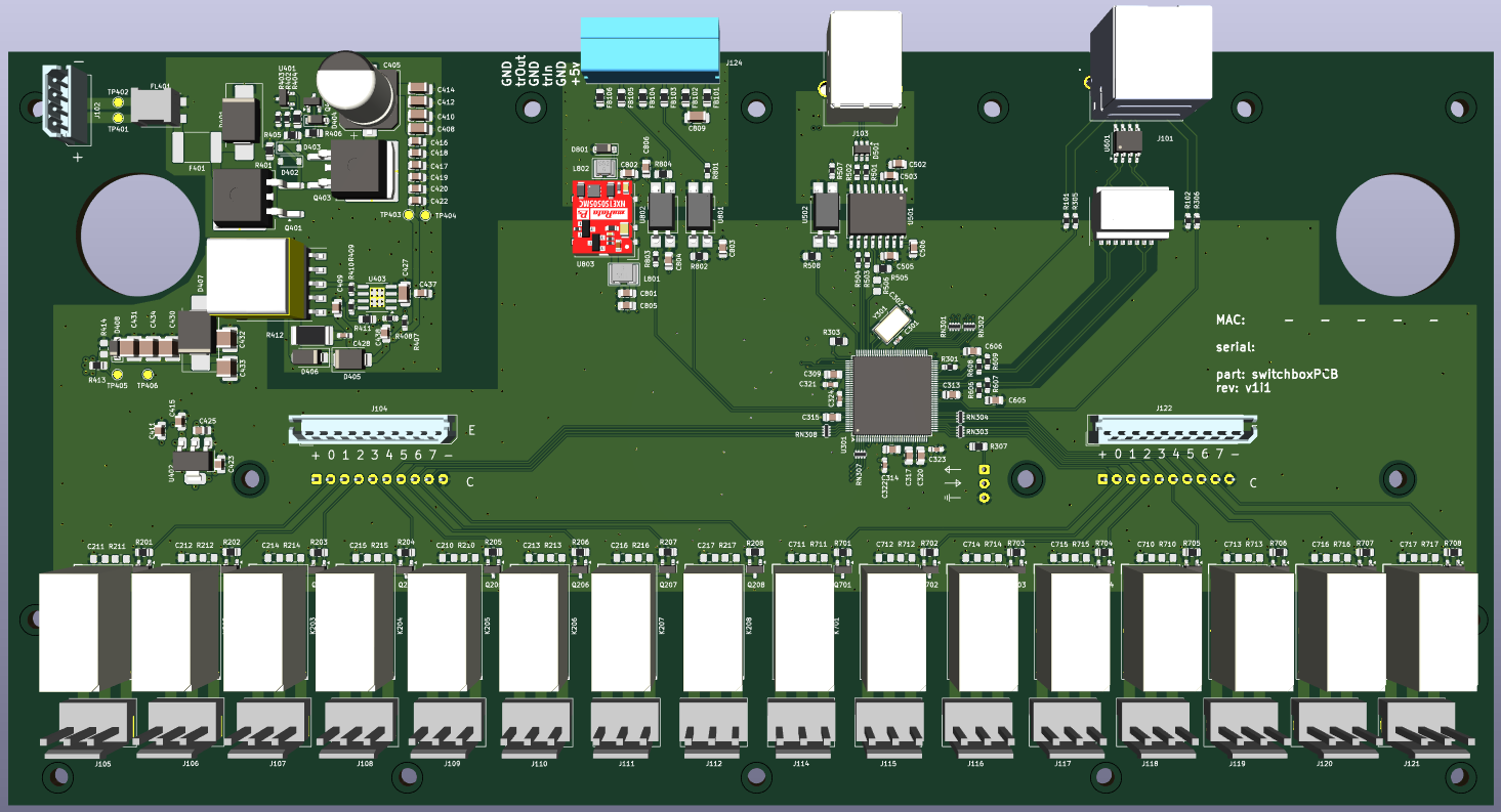
the final 3d rendering of the PCB including the trigger system. this is what finally got built
blog
the current firmware can operate the switches and maintains counts of how many times a given contact has been closed(moved from NC to NO) as well as reporting the status
operation over USB and TCPIP are working
it is planned to add support for static IP addressing
the enclosure is coming along, the base holes have been drilled(but not countersunk) and the rear panel is marked up for the PCB mounted connectors. all front modifications are TODO
both the top and bottom PCBA have been produced
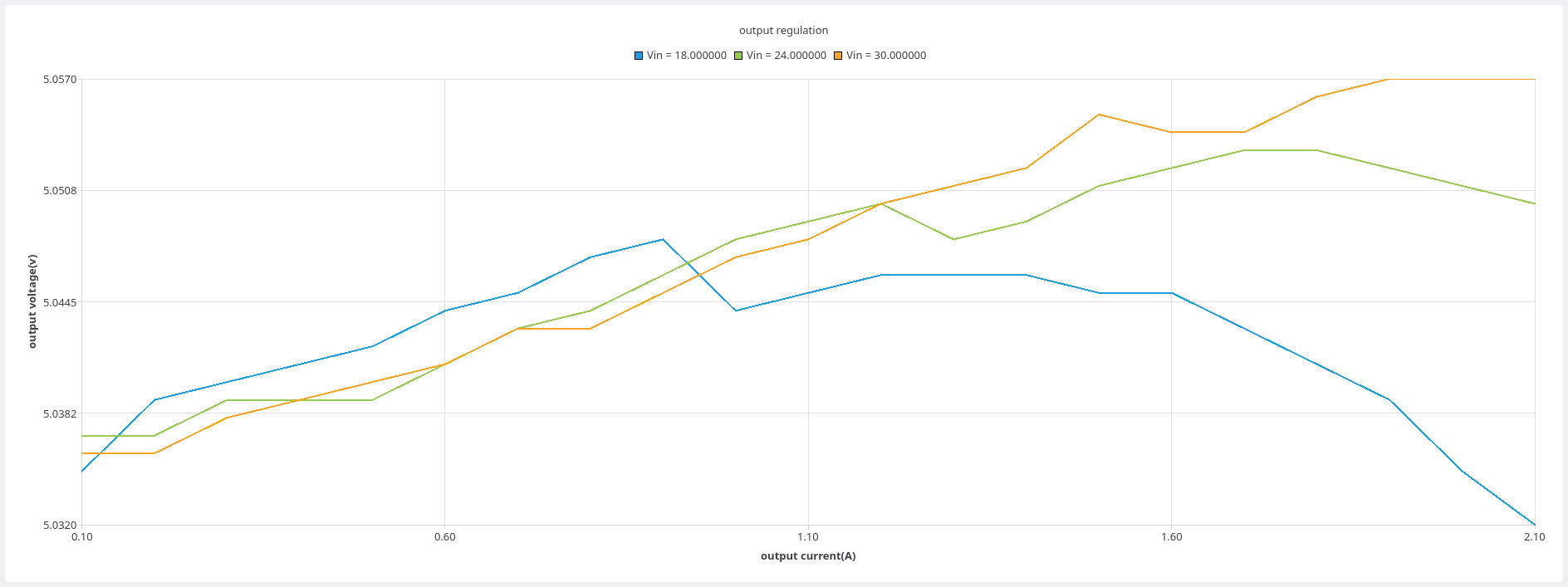
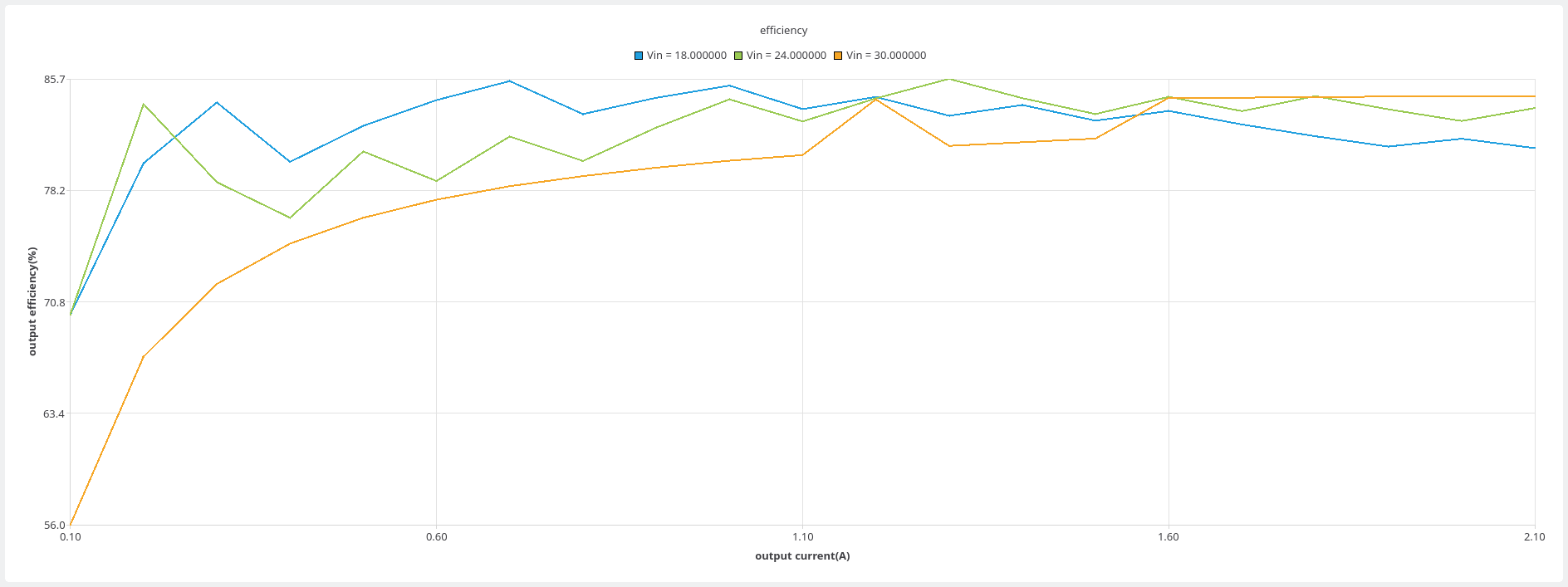
here are some outputs of the power tester. they are regulation and efficiency graphs for the flyback on the switchbox project
the power supply was also successful and had only one(two?) issue(s) which was that the input protection FET gates were not sufficiently protected and i had to fit the two nonpop zeners
the PSU regulates properly over the input range for 110% of the output current range(design=2A, test=2.2A) and is stable for more than 24hrs to within ten millivolts.
the efficiency isnt great, generally being in the upper 70%s but the measurement setup wasnt brilliant, the measured current values from the PSU have not been verified for correctness and may have a large amount of variance, if memory serves there is at least a 2% inaccuracy(was able to measure ~102% efficiency when the tester was in self-verification setup). the graph was also suspiciously spiky
i can finally claim victory over the LT8304!
the USB and ethernet(and therefore also clocking) have been verified before any firmware was flashed as the MCU has a vendor bootloader which may use USB or ethernet; the USB connection showed in dmesg and the ethernet BOOTP requests were visible in wireshark
the trigger subsystem was verified before fitment of the MCU or other comms interfaces and performed as required. later the exported power was loaded and the assembly thermals were reasonable
some firmware work has been done with a functional TCP connection and a couple of commands implemented. the relays have been tested using some temporary commands and perform as expected
so, early signs are good but there are still many unknowns, namely:-
- USB and ethernet at the same time
- full command set
- the chassis connectors are big and will need to be in a 4*8 arrangement, this needs to be drawn and made
- the upper PCBA is still TODO
i may put some form of protection on the ethernet lamps, they dont have any right now
i put the design into aisler to get a RoM cost on the PCB and it is expensive at about £50 per PCB and MOQ of 3 which gives a total PCB cost of £100 per switchBox. this means it needs to be as close to perfect as possible as its very much a oneshot as theres probably about the same in components on the PCBA still, it should be fine...right?
the contact connectors were revisited and actually the chosen part was fine, the model was incorrect but the chosen part was fine and its BoM information is now populated
the PCB is almost done just needing:-
- ethernet
- silkscreen tidying
- routing final look
- DRC
- any additional silkscreen
then it will be on to software! its been a long time coming
there are several component changes to make, they are:-
- longer ethernet connector - there is a 5mm pcb overhang requirement to allow connector access through the chassis wall
- contact connectors - when originally specified, there was insuffiucient bill of materials data and they are fairly tall
i will also need some series resistors as the traces are a bit long...
the mezzanine structure has been scrapped as it would impose too many cutouts, the two levels of PCB will be retained but their stacking will be directly above with wire to board connectors allowing the position offset
this has also triggered a rethink on the internal contact connectors as the existing vertical molex KK are fairly tall and the new layout allows more vertical freedom, the current connectors under review are molex microfit 3.0
front panel connectors are not under review as they still meet all requirements. i did think about instead fitting some D-sub instead but the lower cost connectors dont have the same current rating and this is a non-negotiable feature
- the connectors on the PCB(other than power) are going to be exposed through the chassis wall
- there is a large cutout section to allow stacked PCB to fit against the chassis wall
it might be worth adding better ESD protection now
right now, there are only 32 unrouted nets so changes are probably not going to be major...
looking forward to the layout as thats actually fun